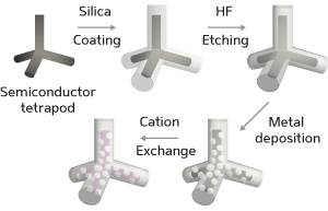
The water-based synthesis and cation exchange reaction of a platinum-decorated semiconductor tetrapod with a hollow silica shell.
Reproduced, with permission, from Ref. 1 © 2012 American Chemical Society
Conversion of water into hydrogen is a fundamental reaction powered by light, but the lack of suitable artificial drivers, or photocatalysts, for this reaction has hampered its commercial development. Platinum-decorated semiconductor nanoparticles are expected to fill this gap; however, production of these tiny particles typically requires high-temperature metal deposition or ultraviolet irradiation techniques in organic solvents. When synthesized in water, as a benign alternative, the particles tend to form clumps during metal deposition. This unwanted agglomeration can now be avoided, thanks to a method developed by a research team at the A*STAR Institute of Materials Research and Engineering in Singapore.
Led by Yinthai Chan, the team used a thin hydrophilic shell of silica to encapsulate individual semiconductor nanoparticles. According to Chan, this encapsulation is the key difference between his team’s method and previous aqueous-phase systems. These systems make the nanoparticles water-dispersible by replacing hydrophobic organic molecules, which bind the as-synthesized semiconductor, with hydrophilic compounds, or ligands. “Our strategy is certainly more robust than those aggregation-free approaches where ligand loss can take place easily upon changes in the solvent environment,” Chan says.
To produce the metal–semiconductor nanostructures, Chan and his co-workers first coated ultra-small, cadmium-containing, semiconducting tetrapods in silica using a surfactant-based emulsion procedure in water (see image). Easily dispersed and stable in aqueous media, the resulting structures displayed a multilayered silica coating that consisted of a hard, tightly woven outer ‘crust’ enveloping a soft, porous inner layer. By selectively removing this inner layer with an acidic etching agent, the team effectively created a hollow shell around each tetrapod. The water-mediated reduction of a platinum precursor, concomitant with its diffusion across the porous shell, generated metal particles that settled on the tetrapod arms.
More importantly, Chan and his team discovered that the encapsulation enabled unprecedented cation exchange reactions which swapped cadmium ions for silver or palladium ions, yielding new platinum–semiconductor tetrapods. “Those nanostructured metal–semiconductor combinations were not readily achievable by established methods, and certainly not via mild aqueous reaction conditions,” Chan notes. Further assessment revealed the presence of an ultrathin film of platinum sulfide at the metal–semiconductor interface. “This unique film is responsible for preserving the metal framework during the cationic exchange of the underlying semiconductor nanostructure,” he explains.
The team is currently investigating the catalytic properties of their tetrapods. “We believe that their stability and efficient light-harvesting abilities may afford a competitive advantage over other metal–semiconductor nanostructures with respect to photocatalysis,” says Chan.
The A*STAR-affiliated researchers contributing to this research are from the Institute of Materials Research and Engineering.


