
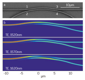
An electron micrograph of the fabricated coupler (top), and the optical energy in the two waveguides (bottom).
Modified from Ref. 1 and licensed under CC BY 4.0 © 2017 G. Chen et al.
A core element of circuits handling optical signals can now be made smaller and simpler, and with functionality over a wider range of wavelengths, because of a mathematical model developed by A*STAR researchers. The new design methodology is expected to have widespread use in photonic integrated circuits and contribute to more compact photonic devices.
Optical signals, such as those transmitted over optical fiber, require photonic elements and circuits to be useful. One of the most important photonic functions is ‘coupling’, which allows the signal to be split into two different paths or used to drive other dependent circuits. Coupling, however, is generally only reliable over a narrow band of wavelengths, demanding a complicated design and fabrication process and bulkier circuits.
To overcome this obstacle to photonic circuit miniaturization, Jun Rong Ong and colleagues from the A*STAR Institute of High Performance Computing, in collaboration with researchers from the Singapore University of Technology and Design, went back to the drawing board to find a simpler approach to designing these critical coupling elements for broadband operation.
“Couplers are the basic building blocks of photonic circuits,” explains Ong. “However, it has been very difficult to try to make them compact, with low power loss and broadband operability, using standard processes.”
A coupler works by running a second optical path, known as a waveguide, alongside the signal path. The optical signal induces a secondary signal in the adjacent waveguide, passing with it some of the signal’s energy. However, the ratio of power splitting changes depending on the wavelength of the signal, so a broadband coupler that provides reliable performance over a wide range of useful wavelengths is something of a holy grail for photonics engineers.
“We distilled the key ingredient that makes a directional coupler a broadband splitter – a combination of straight and bent waveguides – and thoroughly explored and exploited it,” says Ong.
Ong’s team came up with a design methodology based on a mathematical ‘transfer matrix method’ to determine the coupler section lengths, radii, and waveguide cross-sections that would give the desired operation with low wavelength sensitivity. Using this approach, the team designed and fabricated a 50/50 power splitter with a wide bandwidth and length of just 20 micrometers.
“We were able to improve the broadband performance of the photonic power splitter through a simple modification of existing designs, and have achieved a balanced 50/50 output which is difficult by other designs,” Ong says.
The A*STAR-affiliated researchers contributing to this research are from the Institute of High Performance Computing.


