
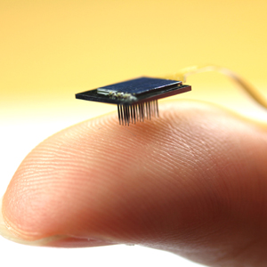
The compact neural probe array consists of a three-dimensional probe array, a custom 100-channel neural recording chip and a flexible polyimide polymer cable.
© 2014 A*STAR Institute of Microelectronics
Neural probe arrays are expected to significantly benefit the lives of amputees and people affected by spinal cord injuries or severe neuromotor diseases. By providing a direct route of communication between the brain and artificial limbs, these arrays record and stimulate neurons in the cerebral cortex.
The need for neural probe arrays that are compact, reliable and deliver high performance has prompted researchers to use microfabrication techniques to manufacture probe arrays. Now, a team led by Ming-Yuan Cheng from the A*STAR Institute of Microelectronics, Singapore, has developed a three-dimensional probe array for chronic and long-term implantation in the brain. This array is compact enough to freely float along with the brain when implanted on the cortex.
The neural probe array needs to be implanted in the subarachnoid space of the brain, a narrow region of 1–2.5 millimeters in depth that lies between the pia mater and dura mater brain meninges. “A high-profile array may touch the skull and damage the tissue when relative micromotions occur between the brain and the probes,” explains Cheng. To avoid this problem, the array should be as thin as possible.
Existing approaches produce low-profile arrays using microscopic electrodes machined from a silicon substrate. These approaches, however, restrict the maximum probe length to the thickness of the substrate and the number of recording electrodes. Other methods generate three-dimensional arrays from silicon-supported two-dimensional probes. Complex and expensive to fabricate, these arrays are too bulky because the silicon support also incorporates the application-specific integrated circuit (ASIC) chip for neural recording.
Cheng and colleagues fabricated two-dimensional probes and inserted them into a thin slotted silicon platform for assembly (see image). To produce a three-dimensional probe array, they joined this assembly to the recording chip. Instead of being aligned, however, the team found that the contacts of the probe electrodes and recording chip were orthogonally arranged with respect to each other, resulting in mismatched planes.
“To solve this issue, the team manufactured a silicon-based connector, or interposer, that electrically linked these components,” says Cheng. “This innovative microassembly effectively controls the final height of the array to within 750 micrometers.”
Compared with commercial neural probes, the new array exhibited competitive electrical properties, including electrode impedance. Moreover, biocompatibility tests showed that the presence of array components did not rupture cell membranes or suppress cell growth. The team is currently refining their approach to integrate the array with a wireless recording chip and make the assembly fully implantable.
The A*STAR-affiliated researchers contributing to this research are from the Institute of Microelectronics.


