
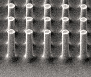
A scanning electron microscopy image of silicon nanopillars on a surface-textured thin film for low-cost solar cells
Silicon is readily available, easy to process, highly stable and non-toxic. It is also one of the best materials for making solar cells. The high quality and purity of silicon needed for fabricating the most efficient silicon-based solar cells, however, has made it difficult to lower production costs for this renewable energy technology. One approach that could reduce costs is to use a microscopically thin film of silicon with a textured surface to enhance light absorption. Navab Singh at the A*STAR Institute of Microelectronics and co-workers have now highlighted several key factors affecting the power conversion efficiency of surface-textured thin-film solar cells and come up with a ‘nanopillar’ design that maximizes light absorption and minimizes production costs.
The best performing thin-film silicon solar cells at present have efficiencies that are about half that of conventional bulk silicon solar cells. “By investigating a variety of appropriate vertical nanopillar designs we can enhance the light-trapping and -collection efficiency of thin films to compensate for the efficiency loss caused by reduced material quality and quantity,” says Singh.
The researchers investigated various factors that might affect the performance of a thin-film solar cell. These factors include the diameter and length of the nanopillar, as well as the spacing between nanopillars (see image). Similarly important is the design of the positively and negatively charged layers in the solar cells that are needed to separate the electrical carriers created by the absorbed light.
The researchers’ simulations showed that the thickness of the negatively charged layer on the outer side of the pillars should be as thin as possible in order to reduce ‘parasitic’ absorption—the annihilation of light-generated carriers before they cross the junction between layers where they would contribute to electrical power generation. They also found that an axial junction design in which the junction between positive and negative layers is confined to the very top of the pillars leads to a higher open-circuit voltage compared with more conventional radial junction structures in which the negative layer wraps around the entire pillars. Yet they found the converse to be true for the open-circuit current.
Singh and his co-workers therefore show that a balance of these factors is needed in order to optimize designs for light-to-power conversion efficiency in surface-textured thin-film structures, which could eventually lead to thin-film silicon solar cells that are able to match the efficiency of the more expensive single-crystalline silicon solar cells.
The A*STAR-affiliated researchers contributing to this research are from the Institute of Microelectronics.


