

Imagine a sheet of paper with a hundred pinholes. You might consider it fragile, but the spacing of those holes makes a big difference. A cluster of several holes would make a weak spot one could easily push a finger through; but if every hole is evenly spaced out, the sheet might hold up as well as a pristine one.
For tungsten disulphide (WS2), the distribution of atom-sized ‘holes’ may have similar effects, as A*STAR researchers recently discovered. Within the semiconductor industry, two-dimensional (2D) sheets of WS2 currently stand out as a promising new material for compact transistors and photodetectors—key parts of smartphones, televisions and other everyday electronics. The catch, however, is that existing methods of processing 2D WS2 often leave S-vacancies—defective ‘holes’ from missing sulphur (S) atoms—on the material’s surface.
“We’ve found in previous studies that such vacancies, even at a relatively low density, can dramatically reduce how well WS2 and other 2D transition metal dichalcogenides (TMDs) transport electrical charges,” said Kuan Eng Johnson Goh, Pillar Director and Senior Principal Scientist at the A*STAR Quantum Innovation Centre (A*STAR Q.InC) and the A*STAR Institute of Materials Research and Engineering (A*STAR IMRE). “These vacancies also trigger chemical reactions with air, oxidising TMDs faster and degrading their electronic performance.”
However, that degradation isn’t always even, as noted by A*STAR IMRE Senior Scientist Fabio Bussolotti and colleagues from A*STAR IMRE, A*STAR Q.InC and the A*STAR Institute of High Performance Computing (A*STAR IHPC). Existing literature has indicated that cracked or uneven TMD sections—which have more closely-packed defects—seemed to degrade faster in air than less-damaged sections.
“This led us to hypothesise a direct relationship between vacancy concentration and air degradation in TMDs,” said Goh. “Previous studies have focused on 2D WS2 flakes with uneven structures and a wide range of defect variations, obscuring a possible connection.”
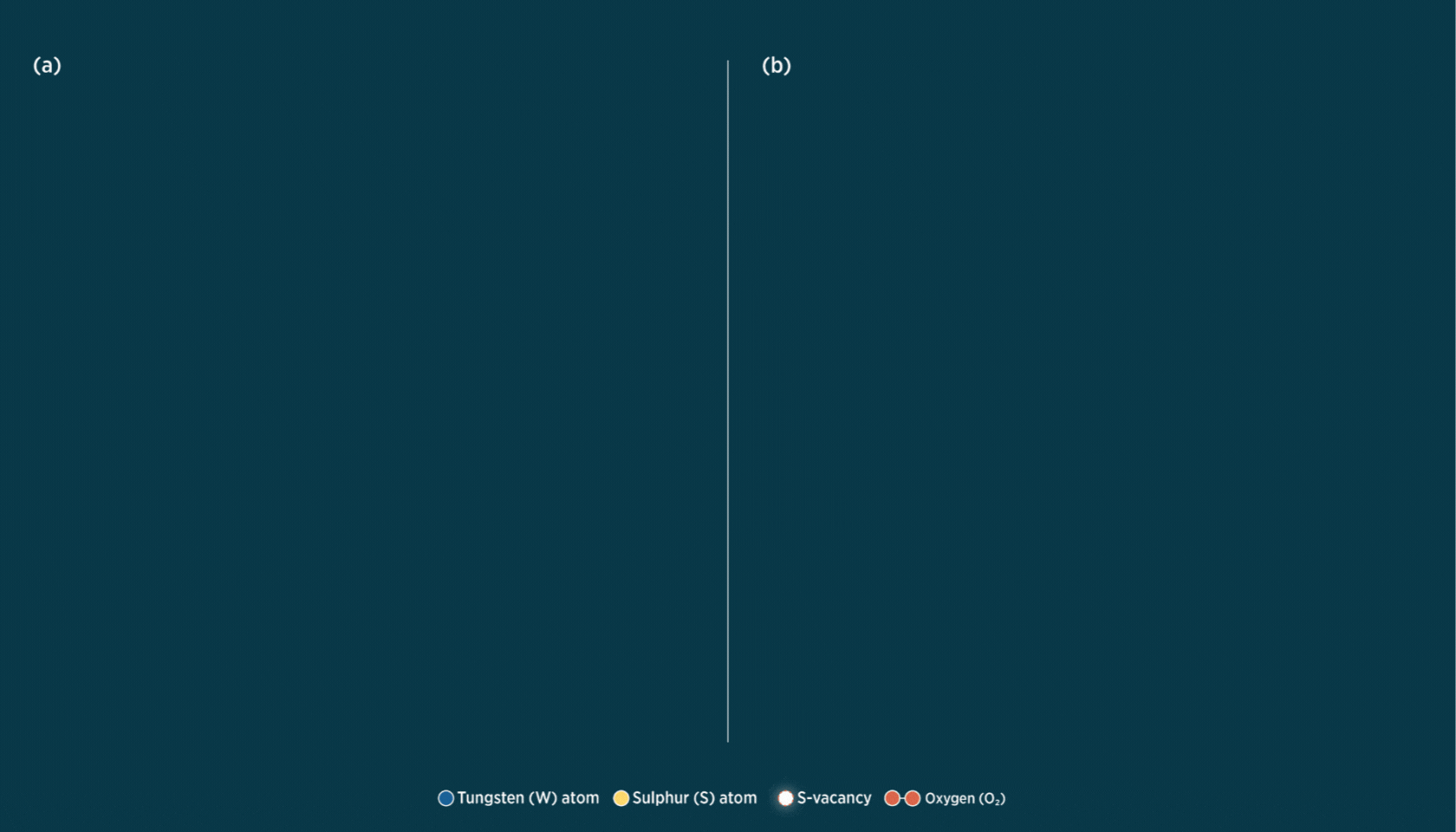
(a) Molecular schematic of low- versus high S-vacancy formations on the surface layer of WS2 single crystals. (b) Molecular schematic of single versus double S-vacancies on WS2 when exposed to atmospheric oxygen (O2). Double S-vacancies tend to absorb O2, causing WS2 to degrade.
To investigate that link, the team cleaved high-quality WS2 single crystals in ultra-high vacuum conditions, creating a surface with minimal defects. They fired high-energy argon ions at the surface to introduce S-vacancies in controlled amounts, then exposed the material to atmospheric conditions typical of factory cleanrooms.
Through X-ray photoelectron spectroscopy and computer simulations, the researchers found that at S-vacancy concentrations over 10 percent, defects were more likely to cluster and lead to WS2 oxidation. Surprisingly, this degradation did not occur when S-vacancies existed in isolated units at a concentration under 10 percent, even at ambient conditions.
“It’s fascinating how WS2’s chemical reactivity can be so deeply affected by a defect site’s physical configuration, a factor quite overlooked to date,” said Bussolotti, the study’s co-corresponding author. “As perfectly defect-free TMD growing methods don’t exist, these findings are encouraging; they can help redefine fabrication strategies that avoid defect clustering, creating more air-stable TMD semiconductors.”
The team recently published a follow-up theoretical paper (Kawai et al., 2025) that generalised their findings to the family of semiconducting TMDs. They have also filed three patents related to the work and are exploring techniques to selectively induce oxidation patterns on 2D TMDs for high-quality devices.
The A*STAR-affiliated researchers contributing to this research are from the A*STAR Institute of Materials Research and Engineering (A*STAR IMRE) and A*STAR Quantum Innovation Centre (A*STAR Q.InC).


